- 您现在的位置:买卖IC网 > Sheet目录323 > DSP56311EVM (Freescale Semiconductor)KIT EVALUATION FOR DSP56311
�� �
�
�Boot-up� Using� the� HI08� Host� Port�
�6.5� Boot-up� Using� the� HI08� Host� Port�
�The� DSP56300� core� has� eight� bootstrap� operating� modes� to� start� up� after� reset.� As� the� processor�
�exits� the� Reset� state� the� value� at� the� external� mode� pins� MODA� /� IRQA,� MODB� /� IRQB� ,� MODC� /� IRQC� and�
�MODD� /� IRQD� are� loaded� into� the� Chip� Operating� Mode� bits� (MA,� MB,� MC� and� MD)� of� the�
�Operating� Mode� Register� (OMR).� These� bits� determine� the� bootstrap� operating� mode.� Modes� C,�
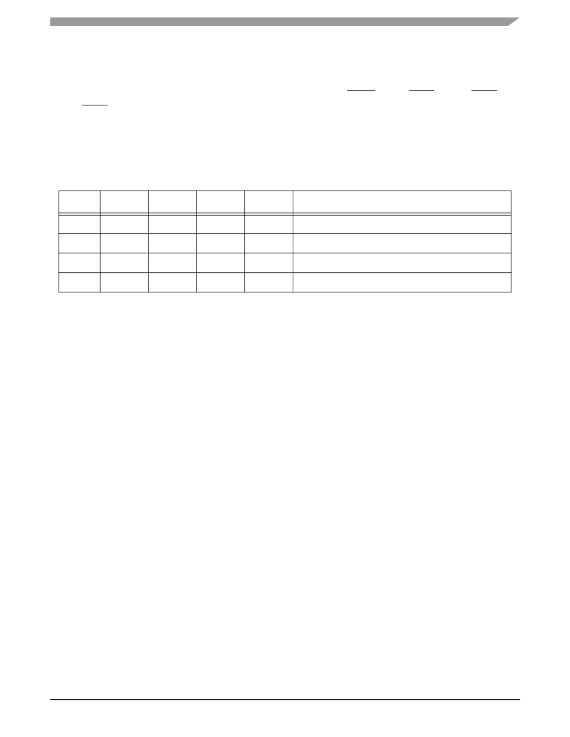
�D,� E� and� F� use� the� HI08� host� port� to� bootstrap� the� application� code� to� the� DSP.� Table� 6-7�
�describes� these� modes.�
�Table� 6-7.� HI08� Boot� Modes�
�Mode�
�C�
�D�
�E�
�F�
�MODD�
�1�
�1�
�1�
�1�
�MODC�
�1�
�1�
�1�
�1�
�MODB�
�0�
�0�
�1�
�1�
�MODA�
�0�
�1�
�0�
�1�
�HI08� Bootstrap� Description�
�ISA/DSP5630x� mode�
�HC11� non-multiplexed� bus� mode�
�8051� multiplexed� bus� mode�
�MC68302� bus� mode�
�The� bootstrap� program� is� factory-programmed� into� an� internal� 192-word� by� 24-bit� bootstrap�
�ROM� at� locations� $FF0000–$FF00BF� of� P� memory.� This� program� can� load� program� RAM�
�segment� from� the� HI08� host� port.� When� any� of� the� modes� in� the� preceding� table� are� used,� the� core�
�begins� executing� the� bootstrap� program� and� configures� the� HI08� based� on� the� OMR� mode� bits.�
�The� bootstrap� program� then� expects� the� following� data� sequence� when� the� user� program� is�
�downloaded� from� the� HI08:�
�1.�
�2.�
�3.�
�Three� bytes� (least� significant� byte� first)� indicating� the� number� of� 24-bit� program� words�
�to� be� loaded.�
�Three� bytes� (least� significant� byte� first)� indicating� the� 24-bit� starting� address� in�
�P-memory� to� load� the� user's� program.�
�The� user� program� (three� bytes,� least� significant� byte� first,� for� each� program� word).�
�Once� the� bootstrap� program� finishes� loading� the� specified� number� of� words,� it� jumps� to� the�
�specified� starting� address� and� executes� the� loaded� program.�
�6.6� DSP� Core� Programming� Model�
�The� DSP56300� core� treats� the� HI08� as� a� memory-mapped� peripheral� occupying� eight� 24-bit�
�words� in� X� data� memory� space.� The� DSP� can� use� the� HI08� as� a� normal� memory-mapped�
�peripheral,� employing� either� standard� polled� or� interrupt-driven� programming� techniques.�
�Separate� transmit� and� receive� data� registers� are� double-buffered� to� allow� the� DSP� and� host�
�processor� to� transfer� data� efficiently� at� high� speed.� Direct� memory� mapping� allows� the�
�DSP56311� core� to� communicate� with� the� HI08� registers� using� standard� instructions� and�
�DSP56311� User’s� Manual,� Rev.� 2�
�Freescale� Semiconductor�
�6-11�
�发布紧急采购,3分钟左右您将得到回复。
相关PDF资料
DSPAUDIOEVMMB1E
BOARD MOTHER DSP563XX
DSPIC30F2010 DEVELOPMENT KIT
KIT DEV EMBEDDED C
DSTRM-KT-0181A
DSTREAM DEBUG AND TRACE UNIT
DSUT1CSU
SURGE SUPPR NETWORK W/GROUND
DTEL2
SURGE SUPPRESSOR PHONE RJ11/RJ45
DV003001
PROGRAMMER PICSTART PLUS 16C/17C
DV164035
MPLAB ICD3 IN-CIRC DEBUGGER
DV164039
KIT DEV PIC24FJ256DA210
相关代理商/技术参数
DSP56311EVMIG_D
制造商:未知厂家 制造商全称:未知厂家 功能描述:DSP56311EVMIG DSP56311EVM Sample Code
DSP56311EVMUM
制造商:未知厂家 制造商全称:未知厂家 功能描述:DSP56311 Evaluation Module Hardware Reference Manual
DSP56311FACT
制造商:未知厂家 制造商全称:未知厂家 功能描述:DSP56311 Higher performance programmable DSP for demanding voice and data applications
DSP56311UM
制造商:未知厂家 制造商全称:未知厂家 功能描述:DSP56311 24-Bit Digital Signal Processor Users Manual
DSP56311UMAD
制造商:未知厂家 制造商全称:未知厂家 功能描述:DSP56311 Users Manual Addendum
DSP56311VF150
功能描述:数字信号处理器和控制器 - DSP, DSC 150Mhz/300MMACS 150Mhz EFCOP RoHS:否 制造商:Microchip Technology 核心:dsPIC 数据总线宽度:16 bit 程序存储器大小:16 KB 数据 RAM 大小:2 KB 最大时钟频率:40 MHz 可编程输入/输出端数量:35 定时器数量:3 设备每秒兆指令数:50 MIPs 工作电源电压:3.3 V 最大工作温度:+ 85 C 封装 / 箱体:TQFP-44 安装风格:SMD/SMT
DSP56311VF150B1
功能描述:数字信号处理器和控制器 - DSP, DSC 24 BIT DSP
RoHS:否 制造商:Microchip Technology 核心:dsPIC 数据总线宽度:16 bit 程序存储器大小:16 KB 数据 RAM 大小:2 KB 最大时钟频率:40 MHz 可编程输入/输出端数量:35 定时器数量:3 设备每秒兆指令数:50 MIPs 工作电源电压:3.3 V 最大工作温度:+ 85 C 封装 / 箱体:TQFP-44 安装风格:SMD/SMT
DSP56311VF150R2
功能描述:数字信号处理器和控制器 - DSP, DSC 24 BIT DSP RoHS:否 制造商:Microchip Technology 核心:dsPIC 数据总线宽度:16 bit 程序存储器大小:16 KB 数据 RAM 大小:2 KB 最大时钟频率:40 MHz 可编程输入/输出端数量:35 定时器数量:3 设备每秒兆指令数:50 MIPs 工作电源电压:3.3 V 最大工作温度:+ 85 C 封装 / 箱体:TQFP-44 安装风格:SMD/SMT